As FPGA design grows in complication and sophistication, the Keysight FPGA dynamic probe, used in conjunction with a Keysight logic analyzer, provides the most effective debugging solution for your FPGA design.
Key Benefits
- Quickly access internal Xilinx FPGA signals
- Make incremental measurements in seconds, without changing design timing
- Access up to 128 internal Xilinx FPGA signals for each pin dedicated to debug
- Measurement can be either in State (synchronous) or timing (asynchronous) mode
Automated Setup
- Automated import of signal names from FPGA design tools
- Auto-pin mapping eliminates mistakes and saves time
Compatibility
- Xilinx FPGA devices: Virtex-5, Virtex-4, Virtex-II Pro, Virtex-II, and Spartan-3
- Requires Xilinx ChipScope Pro or Embedded Development Kit (EDK)
- Probing: flying lead, mictor, samtec, or soft touch probes
- Logic Analyzers: All 16900 Series, 16800 Series, 1680 Series, 1690 Series
Integrated Cockpit for Design and Simulation
The Vivado® Design Suite employs a shared, scalable data model to accommodate the largest programmable logic devices. This single data model is used throughout the implementation process, enabling users to gain visibility into key design metrics such as timing, power, resource utilization, and routing congestion much earlier in the design process. These estimates become progressively more accurate throughout the design flow, enabling faster design closure with fewer iterations.
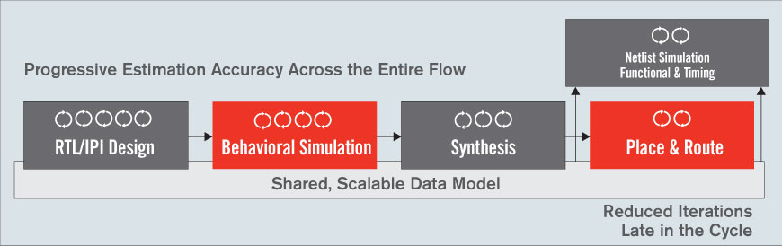
Fig.1 Vivado Design Suite Shared Scalable Data Model
Vivado Design Suite also provides a complete suite of design entry, timing analysis, hardware debug as well as simulation capabilities encompassed in a single state of the art Integrated Design Environment (IDE)
Vivado Design Suite is designed and structured to work off a common data model in memory. This architecture enables extensive cross-probing between design sources, schematic views, hierarchy browsers, design reports, messages, floorplan, and Vivado Device Editor views. This unique capability enables faster debug and timing closure by providing the design feedback specifically to the source of the design issue.
Other solutions are fragmented, while Vivado provides a unified design environment. Where Vivado uses a single shared data model for handling all aspects, competition requires the usage of multiple files written to disk for achieving the same. This leads to multiple different looking interfaces and tools that do not communicate well between each other.
No other solution offer a mixed-language capable simulator that is available as part of their suite. Their simulator offering is either VHDL or Verilog, although with the latest designs having a mixed language simulator is pertinent. Vivado Design Suite also uses a shared waveform viewer for simulation and debug that ensures that there is no learning curve when going from a simulation environment to a hardware debug environment. The Competitive Solution provides two different tools with two different waveforms to achieve the same task
Other solutions are fragmented and thus extremely limited in the cross-probing capabilities that they can provide with their multiple tool offering. The cross-probing capabilities are usually restricted to within the individual tool. Vivado Design Suite provides a complete front to back cross-probing from the different design views, implemented design, synthesized design, timing reports, all the way back to the original RTL coded by the customer.
Comprehensive Hardware Debug
Vivado offers probing methodologies that are intuitive, flexible, and iterative. Users can choose a probing strategy that best suits their design flow:
- RTL design files, synthesized design, and XDC constraint files
- Netlist insertion
- Interactive Tcl or scripts to automate probing
Advanced trigger and capture capabilities
Vivado provides advanced trigger and capture capabilities for detecting complex events, all trigger parameters are accessible during a debug session, users can examine or modify dynamically on the fly without having to recompile the design.
- Integrated into Vivado environment
- IDE integration
- All debug cores available via the IP Catalog
- One-click enablement in IP Integrator
- HDL (VHDL,Verilog) based core instantiation and Synthesized Netlist based core insertion
- Analyze any internal FPGA signal, including embedded processor system buses
- High-level debug with flexible probing capability
- Debug remotely over a network connection
SoC cross trigger between Processor (PS) and Programmable Logic (PL)
This feature provides a means to co-debug an embedded design between PS and PL using the Software Development Kit (SDK) tool suite, IP Integrator, and Vivado logic analyzer. When coupled with a powerful software debugger: the GNU Debugger (GDB) utility, Vivado IP Integrator, and Vivado logic analyzer, this enables users to debug both software and hardware algorithms simultaneously. Designated interface signals are provided between Zynq platform and ILA IP core for seamless co-debug operations.
Enabling hardware read and write in real-time – Hardware AXI Access
Vivado can perform read and write transactions during hardware debugging in real-time. With a new debug IP (JTAG to AXI Master) coupling with easy to use IPI flow, this feature enables users to access data on any AXI IP in a design with a processor-based or non-processor-based design.
Here are some benefits:
- Perform simple peek and poke on certain peripherals in a design
- Write test patterns into memory without recompilation
- Test and calibrate IP via AXI interface
- Check data on any AXI peripherals Vivado Serial I/O Analyzer
Integrated serial I/O analyzer
The Vivado serial I/O analyzer provides a fast, easy, and interactive setup and debug of serial I/O channels in high-speed FPGA designs. The serial I/O analyzer allows you to take bit-error ratio (BER) measurements on multiple channels and adjust high-speed serial transceiver parameters in real-time while your serial I/O channels interact with the rest of the system. It’s a link-based analyzer that enables users to connect from any Transceiver TX to any Transceiver RX. Moreover, TX and RX do not have to be the same architecture. The analyzer also has the ability to auto detect links and allows users to create any custom links, perform 2D eye scan, and sweep transceiver parameters in real-time.
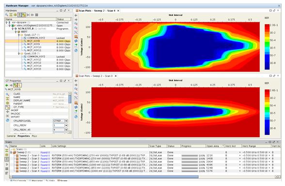
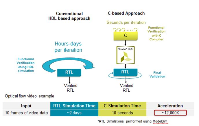
Fig.2 Runtime comparison
Accelerate Verification by >100X with C, C++ or SystemC
Vivado Design Suite System Edition includes Vivado High-Level Synthesis which enables users to create and iterate over their designs in C, C++ or SystemC by leveraging the high simulation speed of this higher level programming language. Using Vivado HLS fixed and industry standard floating-point math.h libraries users can continue to rapidly model and iterate their designs at the C functional specification, and create a target aware RTL architecture based on simple clock period and throughput considerations. Using C as the design and modeling language has a huge impact on simulation run times (1000’s of times faster) as shown by the video example where 10 frames of video data simulated ~12000x faster in C than HDL.
Fonte - Keysight Technologies
Fonte - Xilinx Inc
12 de abril de 2015


